
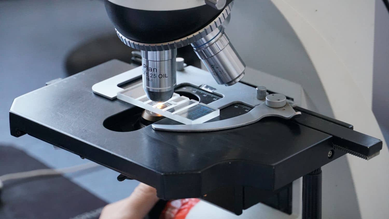
How Scanning Electron Microscopy Works: The Science Behind the Images
Understanding scanning electron microscopy analysis at a technical level helps engineers interpret results more effectively and communicate more precisely with laboratory partners about what a given investigation can and cannot reveal. While the practical applications of SEM are widely discussed, the underlying physics and instrumentation deserve equal attention for anyone relying on this technique for critical quality or failure investigations.
The Basic Principle: Electrons Instead of Light
A scanning electron microscope generates images by scanning a finely focused beam of electrons across a sample’s surface, rather than illuminating it with visible light as an optical microscope does. This fundamental difference is what allows SEM to achieve dramatically higher resolution and magnification than optical methods, since electrons have a much shorter effective wavelength than visible light, allowing the instrument to resolve much finer surface details.
The electron beam is generated by an electron gun, typically using either a heated tungsten filament or a field emission source, and then focused through a series of electromagnetic lenses that narrow the beam to a fine point before it scans across the sample surface in a systematic raster pattern, similar to how an old cathode-ray television built an image line by line.
What Happens When Electrons Hit the Sample
As the focused electron beam interacts with the sample surface, several different signals are generated, each providing different information:
- Secondary electrons are low-energy electrons ejected from the sample’s surface atoms by the incoming beam. Because these electrons originate very close to the surface, they’re particularly sensitive to surface topography, making them the primary signal used for standard high-resolution surface imaging—the images most commonly associated with SEM.
- Backscattered electrons are beam electrons that reflect off the sample rather than being absorbed, with the intensity of backscattering related to the atomic number of the elements present. This makes backscattered electron imaging useful for distinguishing between different materials within a sample based on compositional contrast, even when their surface topography looks similar.
- Characteristic X-rays are emitted when the electron beam causes inner-shell electron transitions within the sample’s atoms, with the specific X-ray energies corresponding to specific elements. This is the signal captured by energy-dispersive X-ray spectroscopy (EDX), allowing elemental identification at the precise location the beam is focused on.
Sample Preparation Considerations
Not every sample can go directly into an SEM without preparation. Non-conductive materials, such as many polymers and ceramics, tend to accumulate electrical charge under the electron beam, which distorts the resulting image through a phenomenon called charging. To prevent this, non-conductive samples are typically coated with an extremely thin conductive layer—commonly gold, platinum, or carbon—applied through a process called sputter coating.
Sample size and vacuum compatibility also matter, since standard SEM operates under vacuum conditions that require samples to be free of volatile materials that could contaminate the instrument or interfere with the vacuum environment. For samples that can’t tolerate standard vacuum conditions, some laboratories offer variable pressure or environmental SEM capability, though this typically comes with some trade-off in achievable resolution.
Understanding Magnification and Resolution Limits
SEM magnification can typically range from around 10x, comparable to a standard optical microscope, up to several hundred thousand times, revealing features at the nanometer scale. However, achievable resolution depends on several factors beyond simply the instrument’s theoretical capability: sample preparation quality, the specific signal being used for imaging, and even the sample material itself all influence how much detail can actually be resolved in practice.
This is worth understanding because higher magnification isn’t always the goal—for many failure analysis applications, moderate magnification that captures the broader context of a fracture surface or contamination pattern provides more diagnostically useful information than extreme close-up imaging of an isolated feature.
From Image to Interpretation
Perhaps the most underappreciated aspect of SEM analysis is that generating a clear image is only the first step—interpreting what that image reveals about a material’s history, failure mechanism, or composition requires experienced analysis. Recognizing whether a fracture surface shows fatigue striations, brittle cleavage, or ductile dimpling, for example, requires familiarity with how these failure mechanisms manifest visually, knowledge built through experience examining many similar cases rather than something derivable from the image alone.
SEM Analysis Services in Malaysia
Understanding the technical foundation of SEM analysis helps manufacturers make more informed decisions about when this technique is appropriate for their specific investigation needs, and what results they can realistically expect.
Alstesting Laboratory Testing service in Malaysia provides SEM imaging alongside EDX elemental analysis, supported by experienced technical interpretation of results. Engineering teams requiring scanning electron microscopy analysis for materials characterization or failure investigation gain access to both the instrumentation and the analytical expertise needed to translate microscopic imaging into actionable engineering conclusions.
Frequently Asked Questions
Does higher magnification always produce better failure analysis results?
Not necessarily. Extremely high magnification narrows the field of view considerably, and for many failure investigations, understanding the broader context of a fracture surface at moderate magnification provides more diagnostically useful information than isolated close-up imaging of a single feature.
Can SEM analyze liquid or wet samples directly?
Standard SEM operates under vacuum, which is generally incompatible with liquid or wet samples unless specialized environmental SEM capability is available; typically, liquid or moisture-sensitive samples require preparation steps such as drying before standard SEM examination.
How does sputter coating affect measurement accuracy?
The thin conductive coating applied to non-conductive samples is generally thin enough not to meaningfully obscure genuine surface features, though extremely fine surface details at the highest magnifications could theoretically be affected, which is why coating thickness is carefully controlled during sample preparation.
Is EDX analysis always performed alongside SEM imaging?
No, EDX is typically added when elemental composition information is specifically needed to answer the investigation’s questions—many SEM examinations focused purely on surface morphology or fracture characteristics don’t require the additional EDX step.